Processes

III – V Processes
III-V Technologies
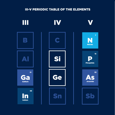
Alloys of the elements found in columns III (B, Al, Ga, In) and V (N, P, As Sb) of the periodic table of elements form a III-V compound. These semiconductors (such as InP, GaAs and GaN) are suitable for a wide variety of applications in high-performance radio frequency and optoelectronic devices due to their superior electronic properties such as high electron mobility, high saturated velocity and large band gap.
MACOM’s European Semiconductor Center portfolio focuses on microwave (uW), millimeterwave (mmW) and terahertz (THz) applications based on GaAs pHEMT and mHEMT and GaN HEMT technologies.
MACOM’s European Semiconductor Center Processes
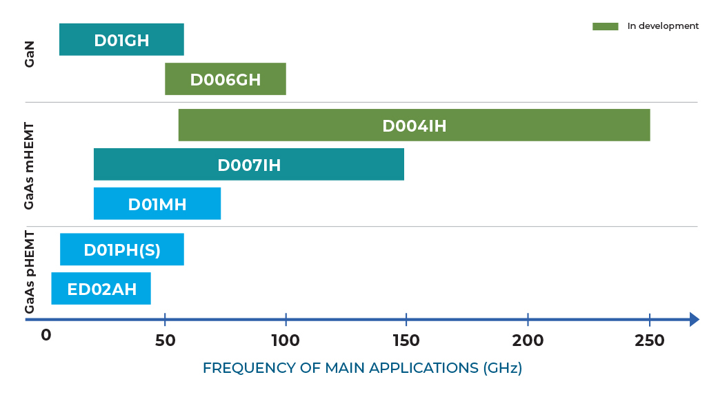
MACOM provides a diverse portfolio of processes using III-V materials. Dedicated to innovation, our team focuses on new technologies which deliver differentiated performance. The foundry offers GaAs pHEMT (EDA02AH, D01PH), GaAs mHEMT (D01MH, D007IH, D004IH) and GaN-on-Si HEMT (D01GH, D006GH) processes for mm-wave applications.
.
GaAs pHEMT Technology
Designed for application from 1 to 40 GHz
LNA, CoreChip, Mixer
Designed for application from 5 to 45 GHz
PA, LNA, Mixer, TWA
GaAs mHEMT Technology
Designed for application from 20 to 75 GHz
LNA, Mixer
Designed for application from 20 to 150 GHz
LNA, Mixer
In development
Designed for application from 60 to 250 GHz
LNA, Mixer
GaN-on-Si Technology
Designed for application from 15 to 50 GHz
HPA, LNA, T/R Chip
Designed for application from 50 to 100 GHz
HPA, LNA, Switch