MACOM UPDATES
- Articles
Designing with Diodes: Protecting Sensitive Components
 Sensitive low noise amplifiers (LNAs) in radar or radio receivers cannot tolerate large input signals without sustaining damage. What’s the solution? Receiver-protector limiter (RPL) circuits, the “heart” of which typically comprises PIN diodes, can be utilized to protect sensitive components from large input signals without adversely affecting small-signal operation.
RPL circuits do not require external control signals. These circuits comprise at least one PIN diode connected in shunt with the signal path, along with one or more passive components, such as RF choke inductors and DC-blocking capacitors. A simple (but possibly complete) RPL circuit is shown below.

When there is no RF input signal or when only a small RF input signal is present, the impedance of the limiter PIN diode is at its maximum value, the magnitude of which is typically in the few-hundreds of ohms or greater. Consequently, the diode produces a very small impedance mismatch and correspondingly low insertion loss.
When a large input signal is present, the RF voltage forces charge carriers into the PIN diode’s I layer, holes from its P layer and electrons from its N layer. The population of free charge carriers introduced into the I layer lowers its RF resistance, which produces an impedance mismatch as seen from the RPL circuit’s RF ports.
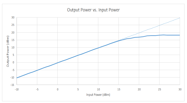
This mismatch causes energy from the input signal to be reflected to its source. The reflected signal, in concert with the incident signal, produces a standing wave with a voltage minimum at the PIN diode since it temporarily presents the lowest impedance along the transmission line. There is a current maximum collocated with every voltage minimum along the transmission line. This current flows through the PIN diode, enhancing the population of free charge carriers in the diode’s I layer, which results in lower series resistance, a greater impedance mismatch and a “deeper” voltage minimum. Eventually the diode’s resistance will reach its minimum value, which is determined by the design of the PIN diode and the magnitude of the RF signal. Increases in the RF signal amplitude force the diode into heavier conduction, thus further reducing the diode’s resistance until the diode is saturated and produces its lowest possible resistance. This results in an output power vs. input power curve as shown below.
After the large RF signal is no longer present, the diode’s resistance remains low (and its insertion loss remains large) if the population of free charge carriers in the I layer is large. Upon cessation of the large RF signal, the population of free charge carriers will decrease by two mechanisms: conduction out of the I layer and recombination within the I layer. The magnitude of the conduction is determined primarily by the DC resistance in the current path external to the diode.
The rate of recombination is determined by several factors, including the free-charge-carrier density in the I layer, the concentration of dopant atoms and other charge-trapping sites in the I layer, etc. Due to the required parameters of the diodes, the greater the RF signal which a PIN diode can safely handle, the longer its recovery time to low insertion loss will be.
The properties of the I layer of the PIN diode determine how this circuit performs. The I layer’s thickness (sometimes referred to as its width) determines the input power at which the diode goes into limiting – the thicker the I layer, the higher the input-referred 1 dB compression level (also known as the threshold level). The thickness of the I layer, the area of the diode’s junction and the material of which the diode is made determine the resistance of the diode as well as its capacitance. These parameters also determine the diode’s thermal resistance.
The simplest implementation of a PIN RPL circuit comprises a PIN diode, an RF choke inductor and a pair of DC blocking capacitors. The RF choke inductor is critical to the performance of the RPL circuit, with the primary function to complete the DC current path for the PIN diode. When a large signal forces charge carriers into the diode’s I layer, a DC current is established in the diode. If a compete path for this DC current is not provided, the diode’s resistance cannot be reduced, and no limiting can occur. This current will flow in the same direction as a rectified current would flow, but it is not produced by rectification.
Implementation of the choke inductor in the RPL circuit can be challenging, since inductors are the least ideal of the components in the RPL circuit. Inductors all have series and parallel resonances due to their inductance and their parasitic inter-winding capacitance. Care must be taken to ensure that series resonances do not occur within the operating frequency band. Additionally, the choke’s DC resistance must be minimized in order to reduce the recovery time of the RPL circuit.
Note: the DC blocking capacitors are optional. They are only necessary if there are DC voltages or currents present on the input or output transmission lines which might bias the PIN diode.
A Practical Example
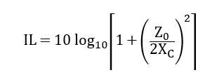
Assume the maximum input power which an LNA can tolerate is 15 dBm. This power level sets the requirement for the I layer thickness of the PIN diode in the RPL circuit, which in this case is approximately 2 microns. A designer can then determine the acceptable capacitance of the PIN diode from the frequency of the RF signal and the maximum acceptable small-signal insertion loss. If they assume the RPL operates in X Band and the maximum acceptable insertion loss is 0.5 dB, then the maximum capacitance of the diode can be calculated.
The insertion loss (IL) in decibels of a shunt capacitance is given by:
We can solve that equation for C:
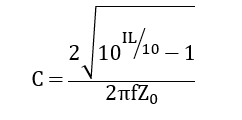
For f = 12 GHz, IL = 0.5 dB and Z0 = 50 Ω, C = 0.185 pF.
Along with the I layer thickness, this value of capacitance will determine the area of the diode’s junction.
The combination of thin I layer and small junction area creates a diode which has relatively high thermal resistance, which cannot dissipate very much power without forcing the junction temperature to exceed its maximum rated value of 175 °C. Typically, a 2 micron diode with 0.185 pF capacitance can safely handle a large CW input signal of around 30 to 33 dBm. A larger signal can potentially damage or immediately destroy this diode due to the Joule heating produced by the current flowing through the diode’s electrical resistance.
PIN diode RPL circuits reliably protect sensitive components like low noise amplifiers in radar or radio receivers from large incident signals. For RPL applications which require very low flat leakage output power but high input power handling, additional diode stages and other circuit enhancements can be added at the input side of the RPL circuit.
Members of MACOM’s applications engineering team are ready to help you select the optimal diodes and circuit topologies for your RPL application. For more information on MACOM’s solutions, visit: https://www.macom.com/diodes